Facilities

“Important: Please mention the instrument name in the payment voucher”

The nanotech research facility at PSGIAS consists of state-of-art equipments for nano material synthesis, characterization and fabrication. Advanced high tech infrastructure and instruments for research in the field of nanoscience and nano technology are situated at various laboratories.

Revised analysis charges for testing and consultancy


Job request form

Material Characterization

Download Rules and Charges

Contact : Dr. Anuradha M. Ashok.
Mail : anu@psgias.ac.in,hrtem@psgias.ac.in

The JEOL JEM 2100 High Resolution Transmission Electron Microscope (HRTEM) provides one of the best-in-class solutions to problems in diverse fields ranging from Materials Science to Biology. This microscope enables to view lattice resolution of 0.14 nm and point-to-point resolution of 0.19 nm with the following features

SPECIFICATION:
  • Electron Source : LaB6.
  • Working Voltage : 200 kV and 80 kV.
  • CCD Camera : Gatan Orius SC200 (Resolution 2K x 2K).
  • Detectors : EDS (Oxford Inca X-Sight
  • Imaging Scale : 1μm, 500nm, 200nm, 100nm, 50nm, 20nm, 10nm, 5nm and 2nm.
Operations
  • Bright Field (BF) and Dark Field (DF) imaging,
  • High Resolution Electron Microscopy (HREM),
  • Selected Area Electron Diffraction (SAED),
  • Energy Dispersive X-ray Spectroscopy (EDS),
  • Nano Beam Diffraction (NBD),
  • Convergent Beam Electron Diffraction (CBED).
nanoresearch

TEM Specimen Preparation Facility

The HRTEM facility has a full range of Gatan sample preparation equipments for TEM specimen preparation in addition to the basic facilities such as carbon and/or formware coated copper grids.

Minitom low speed diamond saw

To slice the sample up to 500 micron

Ultrasonic disc cutter

To make 3mm diameter discs from brittle samples

Dimple grinder

To make a dimple in the sample having thickness around 15 micron at the centre

Precision Ion Polishing System (PIPS) with Liquid
Nitrogen cold stage and auto terminator

To get the sample thickness upto 10nm

Twin-Jet Electro-polisher

Electro-polishing is a well-known technique, mostly used to prepare (inter)metallic samples, because these materials are conducting, too soft for crushing, and easily damaged by conventional ion milling

TEM specimen cross section kit

To prepare cross section samples

Specimen lapping kit

To grind the sample

Download Rules and Charges

Contact : Dr. K K Venkataraman, kkv@psgias.ac.in

The instrument is capable of performing multimode operations especially for analyzing surface characteristics with high precision and resolution. It is possible to carry out experiments in air, vacuum as well as in liquids in controlled environment. The added new generation electronics provides operations even in high-frequency modes.

AFM Imaging: Contact / Semi contact mode
In air and vacuum
  • Scanning Tunneling Microscopy (STM)
  • Lateral Force Microscopy (LFM)
  • Phase Imaging, Force Modulation
  • Magnetic Force Microscopy (MFM)
  • Electrostatic Force Microscopy (EFM)
  • Spreading Resistance Imaging (SRI)
  • Scanning Capacitance Imaging (SCI)
  • Scanning Kelvin Probe Microscopy (SKM)
  • Heating Stage Operations
  • Adhesion Force Imaging
  • AFM Nanolithography
  • Nanosclerometry with AFM-Nanoindentation
In Liquid
  • Contact AFM/LFM/Adhesion Force Imaging/Force Modulation, Phase Imaging
  • AFM Nanolithography
  • Electrochemical AFM/STM Imaging

Bench-top Scanning Probe Microscope AFM/STM (Nanosurf)

Nanosurf AFM and STM is user friendly, compact instrument used for surface characterization of nano and microscale materials in material science and life science disciplines which supports

  • Contact mode AFM imaging
  • STM imaging
bench

Download Rules and Charges

Contact : + 91 – 422 – 434 4000, EXTN : 4321
Email : sem@psgias.ac.in
Dr. Anuradha M Ashok – anu@psgias.ac.in
Scanning electron microscopy (EVO 18) with cryo facility for sensitive samples

Scanning electron microscope (SEM) is a non-destructive technique that uses an electron beam to analyze surface details down to nano-scale. PSGIAS has EVO 18 model with low vacuum facility and ALTO 1000 cryo attachment for biological, hydroscopic and sensitive samples.

Environmental

Download Rules and Charges

Contact : xrd@psgias.ac.in
Dr. Anuradha M Ashok. – anu@psgias.ac.in

Empyrean, Malvern Panalytical

The Empyrean Series III Diffractometer is the first intelligent,multipurpose diffractometer with innovative features which allows the largest variety of measurements.
The Bragg-Brentano High Definition High Intensity Incident Beam Optics is a unique optical module from Malvern Panalytical analysis of Powder, Nano Material & Thin Film without any change over
Bragg-Brentano HD is a Special Unique
incident beam optic offering from us for Bragg-Brentano Focusing Geometry & parallel Beam Geometry measurements with an energy resolution of about 450 eV with the high speed detector offered, replacing the incident beam Ni Beta-filter With improved peak-to-background ratio and better low angle
performances.

X-Ray sources: Cu Kα (λ = 1.54 Å) (default)

Techniques
  • Rapid powder X-ray diffraction (PXRD): Powder XRD done at standard angular resolutions is rapid and gives precise data with high intensity peaks. Very high angular resolution scans are also possible. Sample type: powder, metallic, thin films, liquid and polymer samples
  • Grazing incidence X-ray diffraction (GIXRD) : or thin films: Grazing incidence x-ray diffraction is used to analyse specifically thin crystalline films (20-200nm depending on mean atomic number) on polished, flat surfaces. It is possible to deal with multiple films to a limited extent
  • 2D scan to view the diffraction patterns in two dimensional texture analysis using pole figures for metallic samples
Software packages available in our facility
  • Data collector(to collect the XRD spectrum data)
  • Data viewer (to visualize the XRD spectrum data)
  • X’Pert Highscoreplus(processing of XRD spectrum, Profile fitting, Williamson Hall plots and Rietveld refinements)
  • X’pert texture (for texture analysis using pole diagrams)
  • XRD 2D scan (to visualize the patterns in 2D)
  • ICDD PDF-2 (Crystallographic database)
Raman

Download Rules and Charges

Faculty In-charge : Dr. P. Biji, pbm@psgias.ac.in

Confocal Raman Microscope with AFM imaging (WiTec alpha 300, Germany) installed at PSG Institute of Advanced Studies is an integrated system with high resolution nanoimaging capability. It can be mainly used for chemical analysis at sub-micrometer scale.

The confocality of the optical design facilitates excellent depth resolution and makes the generation of 3D Raman images and depth profiles easily with a Raman Spectral range of 50 cm-1 – 4000 cm-1. Confocal micro-Raman spectroscope has features such as, Single-point spectra acquisition, Single-point depth profiling and 3D imaging and depth profiling. The advantage of an integrated system with a combination of ultra-high topographic and lateral resolution of AFM with Raman spectroscopy provides a more comprehensive understanding of the samples; not only the chemical information, but also structural and topographic information acquired at the same time and from the same sample area.

The system is integrated with a motorized stage as well as high resolution piezo XYZ mapping Stage with AFM imaging capability. The instrument is equipped with 355 nm and 532 nm lasers as UV Excitation Laser source for PL analysis and VIS Excitation Laser source for Raman analysis respectively. Using optical pre-inspection by means of various illumination and detection techniques (e.g. bright field, dark field, polarization, fluorescence, etc.) the area of interest for the AFM/Raman imaging can be easily determined. The system is capable of measuring the Raman spectra of wide variety of samples including amorphous, crystalline, polymer or liquid/biological samples.

Raman

Download Rules and Charges

TEMPERATURE DEPENDENT HALL MEASUREMENTSYSTEM

Contact : hall@psgias.ac.in,
Dr. Anuradha M Ashok – anu@psgias.ac.in

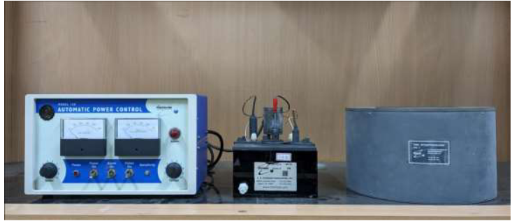
Hall Effect Measurement Systems plot concentration versus temperature, mobility versus temperature, resistivity versus temperature, conductivity versus temperature, and Hall coefficient versus temperature. The HMS3000 & temperature controller HT55T5 includes software with I-V curve capability for checking the ohmic integrity of the user made sample contacts. The systems ramp to each user defined temperature, stabilize, makes the measurement and then plots the various temperature dependent material electrical properties.

Instrument : HMS 3000 from Ecopia Corp, South Korea with high temperature sample stage HT55T5 with a magnetic field of 0.5Tesla

Features
  • Low and high resistivity measurement capability, bulk and sheet carrier concentration and mobility, Hall coefficient in semiconductors
  • DC measurement modes
  • van der Pauw and Hall measurements
  • Measurement from room temperature to 673K
nanoresearch

Download Rules and Charges

Contact:Dr.B.Geetha Priyadarshini, bgp@psgias.ac.in

Nanotech research innovation and incubation centre at PSGIAS has commissioned Keysight B1500A parametric analyzer with Cascade EPS150 Triax EDU probe station for device characterization.

  • 4 Mid power source monitor unit.
  • Capacitance measurement unit.
  • CMOS Transistor: Id-Vg, Id-Vd, Vth, breakdown, capacitance, QSCV, etc.
  • Bipolar Transistor: Ic-Vc, diode, Gummel plot, breakdown, hfe, capacitance, etc.
  • Discrete device: Id-Vg, Id-Vd, Ic-Vc, diode, etc.
  • Memory: Vth, capacitance, endurance test, etc.
  • Power device: Pulsed Id-Vg, pulsed Id-Vd, breakdown, etc.
  • Nano Device: Resistance, Id-Vg, Id-Vd, Ic-Vc, etc.
  • Reliability test: NBTI/PBTI, charge pumping, electro migra-tion, hot carrier injection, J-Ramp, TDDB, etc.
PARAMETRIC ANALYZER
Measurement capabilities
  • Current-voltage (IV) measurement capabilities of spot, sweep, sampling and pulse measurement in the range of 0.1 fA – 1 A / 0.5 μV – 200 V
  • AC capacitance measurement in multi frequency from 1 kHz to 5 MHz and Quasi-Static Capacitance-Voltage (QS-CV) measurement capabilities
  • Advanced pulsed IV and ultra-fast IV measurement capability from minimum 5 ns sampling interval (200 MSa/s)
  • Up to 40 V high voltage pulse forcing for non-volatile memory evaluation
  • 15-inch wide touch screen supports intuitive GUI opera-tion of the EasyEXPERT group+
  • Windows Embedded Standard 7 (WES7)
  • GPIB, USB, LAN interfaces, and VGA video output port
  • Multi-frequency AC impedance measurement supports CV (capacitance versus voltage), C-t (capacitance versus time) and C-f (capacitance versus frequency)measurement
  • Capacitance measurement frequency range of 1 kHz to 5 MHz
  • 150 mm manual probing solution for low-noise measurements
  • 4 probes with industrial standard positioners
  • 100X magnification microscope with camera output
  • Supports single chip and wafers
cviv
cviv

Download Rules and Charges

SIMULTANEOUS THERMAL ANALYZER

Contact : tgdsc@psgias.ac.in,
Dr. Anuradha M Ashok – anu@psgias.ac.in

TGA : mass changes, temperature stability, oxidation/reduction behavior, decomposition, corrosion studies, compositional analysis and thermokinetics.

DSC : melting/crystallization behavior, solid-solid transitions, polymorphism, degree of crystallinity, glass transitions, cross-linking reactions, oxidative stability, purity determination, specific heat and thermokinetics

Simultaneous Thermal Analysis generally refers to the simultaneous application of Thermogravimetry (TGA) and Differential Scanning Calorimetry (DSC) to one and the same sample in a single instrument.The advantages of the instrument are: The test conditions are perfectly identical for the TGA and DSC signals (same atmosphere, gas flow rate, vapor pressure on the sample, heating rate, thermal contact to the sample crucible and sensor, radiation effect, etc.).

Instrument : STA449 F3 Jupiter from Netzsch, Germany

Sample quantity : 5 mg

Atmosphere : Nitrogen, Air, Argon

Heat ramp :20 K/min

Temperature :Upto 773 K (Aluminium crucible), 1473 K (Alumina crucible)

nanoresearch

Download Rules and Charges

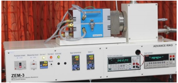
ZEM3 M10 simultaneous Seebeck and electrical resistivity measurement system:

Contact : Dr. Anuradha M Ashok – anu@psgias.ac.in ,

ZEM 3 M10 is capable of carrying out simultaneous measurements of Seebeck coefficient and electrical resistivity of thermoelectric materials with high reproducibility. It can measure a wide range of samples including semiconductors, oxides and metals at a temperature range between 50 oC to 1000 oC.
The sample holder uses a unique balance contact mechanism, permitting measurement of high reproducibility. V-I plot measurement can be made to judge if the lead is in intimate contact with a set sample. The system automatically examines whether the contact of the probes with a sample ohmic or not, and finds and uses the best value of electric current to determine the resistivity of the sample without influence of heat transfer.Measurement is controlled by a computer, permitting automatic measurement with each temperature difference at a specified temperature and elimination of dark electromotive force.

Measurement technique Seebeck Coefficient: Static DC method

Electric Resistance: Four- Probe method

nanoresearch

Download Rules and Charges

Contact : Dr. D. Gnanaprakash, dgp@psgias.ac.in

Download Rules and Charges

Contact : Dr. S. Chandirasekhar, scs@psgias.ac.in

The Ocean HDX spectrofluorometer uses a superior optical bench design, optimized components and precision engineering to maximize optical resolution, increase throughput, reduce stray light and maintain thermal stability for integrated, industrial and research applications. HDX has a back-thinned CCD array and “High Definition Optics” design to deliver an exceptional level of spectral performance for a compact, UV-Vis-NIR spectrometer.

A Charge Coupled Device (CCD) is a highly sensitive photon detector. It comprises numerous light-sensitive segments referred to as pixels, allowing for the construction of images within the region of interest. Operating on silicon technology, a CCD functions as a multi-channel array detector capable of capturing UV, visible, and near-infrared light.

  • Advantages : While a typical spectrofluorometer usually measures emissions from 200 nm to 800 nm, the Ocean HDX extends this range to 200 nm to 1100 nm.
  • Brand: OCEAN INSIGHT
  • Spectrometer Model: OCEAN-HDX-XR
  • Monochromator: MARUTEK XM-100-CC
  • Spectral Range: 200 nm – 1100 nm
  • Sample holder: Liquid, Film
  • Sample Quantity: 2 mL/500 mg & Film: 1cm x 1cm

Fabrication/Processing Facilities

Download Rules and Charges

Download Rules and Charges

Durham Magneto Optics Ltd
Contact: Dr. B. Geetha Priyadarshini , bgp@psgias.ac.in

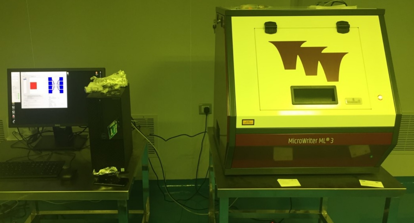
The MicroWriter ML® is photolithography machine designed for rapid prototyping and small volume manufacturing in R&D laboratories and clean rooms. MicroWriter ML®3 is is a compact, high-performance, direct-write optical lithography machine .

The machine is placed in yellow class 1000 clean-room.

Key features and specifications:
  • 195mm x 195mm maximum writing area.
  • 230mm x 230mm x 15mm maximum wafer size.
  • 0.6µm, 1µm, 2µm and 5µm resolutions across full writing area.
  • Automatic selection of resolution via software – no manual changing of lens required.
  • 385nm long-life semiconductor light source, suitable for broadband, g-, h- and i-line positive and negative photoresists (e.g. S1800, ECI-3000, MiR 701, SU-8).
  • XY interferometer for precise motion control. Extremely fast writing speed – up to: 20mm2/minute (0.6µm resolution), 50mm2/minute (1µm resolution), 100mm2/minute (2µm resolution) and 180mm2/minute (5µm resolution). These allow a typical 50mm x 50mm area combining critical and non-critical areas to be exposed in under 30 minutes or a typical 100mm x 100mm area to be exposed at 2µm resolution in under 2 hours.
  • Autofocus system using yellow light which automatically tracks surface height variation during exposure, compensating for bowed or inclined substrates and surfaces with highly irregular topography. No minimum wafer size. High quality infinite conjugate optical microscope camera with x3 aspheric objective lens and x5, x10 and x20 Olympus plan achromatic objective lens and yellow light illumination for alignment to lithographic markers on the wafer (±0.5µm 3σ alignment accuracy).
  • Automatic changing between microscope magnifications via software – no manual changing of lens required. Additional x4 digital zoom can be selected in software. Grey scale exposure mode for 3-dimensional patterning (255 grey levels).
  • Software API for external interfacing and control.
  • 100nm minimum addressable grid; 20nm sample stage resolution.
nanoresearch

Download Rules and Charges

Laboratories

Faculty In-charge : Dr. B. Geetha Priyadarshini

75 sq. m. of Class 10000 and 170 sq. m. of Class 1000 clean room housing facilities for hybrid renewable energy systems, Flexible electronics, smart textiles and health care devices.

Equipments
Multi source Physical Vapour Deposition system and parylene coater integrated in Glove Box

Custom built for developing composite thin film or multilayer films with co-sputtering and co-evaporation of metals, organics and oxides with substrate heating facility with the following sources integrated in DANVEC glovebox commissioned in class 10000 clean room. Parylene coater provides conformal coating of fabricated devices to protect the device from environmental contamination as well as incorporates biocompatibility for implantable devices.

  • Thermal evaporator
  • E-Beam evaporator
  • DC sputtering
  • RF Sputtering
  • RADAK sources

Parylene coater
  • RF and DC sputtering/pulsed DC sputtering with 3″ target with co-sputtering capability
  • Radak(2 numbers) with Alumina crucible upto 1250 deg.C
  • Thermal (2 numbers) with boat and filament type
  • E-beam with six slots for source material with Thermal and RADAK co-evaporation
  • Parylene coater provides conformal coating

Parametric analyzer with probe station

ICPCVD

  • Rapid Thermal processor
  • Wet processing fumehood
  • Reactive Ion etcher
  • Nano imprint lithography

MicroWriter ML3 Pro: a direct-write photolithography machine for rapid prototyping in R&D

Key features:

  • 195mm x 195mm maximum writing area
  • 230mm x 230mm x 15mm maximum wafer size
  • 0.6µm, 1µm, 2µm and 5µm minimum feature sizes across full writing area. 0.4um minimum feature size available as an option
  • Automatic selection of minimum feature size via software – no manual changing of lens required
  • 385nm long-life semiconductor light source, suitable for broadband, g-, h- and i-line positive and negative photoresists (e.g. S1800, ECI-3000, MiR 701, SU-8). Replacement 365nm lightsource available as option for improved performance with SU-8 photoresist

Faculty In-charge : Dr.SebinDevasia

The Solar Energy at Nanotechnology Research Innovation and Incubation Centre at PSGIAS is on different kinds of solar cells ranging from Crystalline Silicon Solar Cells, CZTSSe based thin film solar cells, Dye Sensitized Solar Cells, Perovskite Solar Cells, Organic Solar Cells, Organic-Inorganic Hybrid Solar Cells. The lab is well equipped with a thermal evaporator in laminar flow hood for Metal, Oxides, Organics and Dielectrics evaporation, Glove Box, Spin Coater, UV Source for Photolithography, Solar Simulator and Keithley Source Meters.

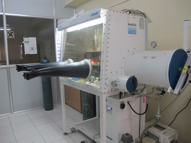
MBRAUN Glove Box for Controlled Atmosphere, used for the fabrication of Dye Sensitized Solar cells, Perovskite Solar Cells, etc

Keithley Source Meters for Current – Voltage Measurement of Solar Cells

Spektrospin Spin Coater – Photoresists & thin films

ABETT Technologies Solar Simulator – Efficiency of Solar Cells

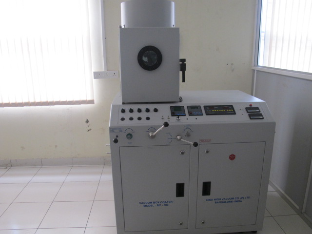
Thermal Evaporator (Box Coater), Hind High Vacuum, Bangalore – Metals, Oxides and Dielectrics Evaporation

Custom made UV Photolithography for Device Patterning

Faculty In-charge : Dr. P. Biji

Keithley High Resistance Meter (Model – 2420 Source meter with 2182A Nanovoltmeter)

is used for the electrical characterization of the conducting/semiconducting thin films. The built-in voltage source simplifies determining the relationship between an insulator’s resistivity and the level of source voltage used. It is well suited for capacitor leakage and insulation resistance measurements, tests of the surface insulation resistance of printed circuit boards, voltage coefficient testing of resistors, gas sensing studies, solar cells studies and diode leakage characterization. Instrument is provided with 2 probe and 4 probe set up for electrical measurements.

High Intensity Ultrasonic Processor (Model-Sonics Vibra cell VC-505)

is used to disperse the materials in a solution phase. The SS velocity horn immersed into the solution produces high frequency vibrations which are used to beak the materials by cavitation process. This process give raise to intense local pressure waves and micro streaming of liquid round the points to collapse. This machine equiped with 500 watts, 20kHz automatic tuning energy monitor, digital wattmeter, microprocessor based programmable LCD screen.

Langmuir-Blodgett Unit (Model – KSV-NIMA LB Medium, Finland)

is used to create, modify and study thin films as monolayer at air-water interface for varied applications. Using this instrument, we can fabricate mono/multilayers of amphiphilic molecules, nanoparticles, nanowires or microparticles that reside at air-water interface. The thin films can be directly transferred onto suitable substrates or device structures.

Spin coating unit (Model-WS-650MZ-23NPP, Laurell Technologies, USA)

is used to coat materials over a substrate of sub micron thickness. Mainly used to make thin films of polymers, colloids, nanomaterials and photoresist etc with uniform thickness. The process involves deposition of small puddle of fluid resin onto the centre of a substrate and then spinning the substrate at high speed. Centripetal acceleration will cause the resin to spread to and eventually off, the edge of the substrate leaving a thin film. The current model is dedicated tabletop device to spin small substrates upto 150 mm diameter with 100-*12000 RPM speed.

Faculty In-charge : Dr. R. Selvakumar
Consultancy and Testing Charges

Nanobiotechnology laboratory is involved in Microbial based bio remediation research, biosensor development, synthesis and application of nanomaterials for water purification, and effluent treatment.

To support the research we have the following facilities
  • Phase Contrast Microscope- Carl Zeiss, Germany
  • Lass II type II Biosafety cabinet- Clean Air, India
  • High Speed Refrigerated centrifuge (30K) – Sigma, Germany
  • Electrophoresis units – Genei, India
  • Gel documentation unit – Gelstan 1312 F-Advanced, India
  • Ion selective electrodes for fluoride, nitrate and ammonia detection (Orion, USA)
  • Ion chromatography system- Metrohm, Switzerland
  • Rocking Shaker- ORBITEK ® – LE, India
Instruments
Gel documentation unit – Gelstan 1312 F-Advanced.

Wavelength: 312nm & 360 nm, Epi white illumination, Ethidium Bromide Filter-CCD camera 1D image analysis and colony counting software

Electrophoresis units – Genei, Bangalore

Vertical, Submarine gel electrophoresis units with Power packs

Class II type II Biosafety cabinet- Clean Air, Chennai

Cleanair Class II Type A2 Biohazard Safety Cabinet; Model No: CBS 1200-II-A2 Working Size: W 1200 x D 600 x H 600 mm; Along with Virus Burnout unit; 70% re-circulation and 30% exhaust with incinerations; Particle Retention- 0.3 Micron & above

Phase Contrast Microscope- Carl Zeiss, Germany

Primo Star” with Digital Photo-micrography attachment includes Digital Camera Adapter P95 M37/52×0.75 for “Primo Star” and Digital Camera- Canon 10.0 megapixels

Dry Bath- Rivoteck, India

Temperature range ambient to 110° C controlled to + 0.2° C by solid – state time proportional temperature controller cum digital display

Peristaltic pump- Rivoteck, India

6 – 60ml/h (in I.D.1/O.D.3 tube) during running with flow indicator.

Temperature Controlled Shaker Scigenics, India

ORBITEK ® – LE
With Universal Tray and 25 Clamps to hold 250 ml Flasks
Temp range: 15 °C to 60 °C)

Rocking Shaker

Rockymax, Tarsons Maximum RPM (< 50), i.e. shacking speed at maximum strokes per minute (Digital). Platform size 30x30cm; timer: 99hrs 99min (Digital).

Refrigerator

230 Ltrs, Double Door, Frost Free LG Model: GL- 241NT5 with stand

Deep freezer (-20 °C)

Cell frost -Model No: BFS 150; Capacity : 148 liters Dimension: 20x24x48 (WxDxH); Temperature: – 17 °C to -24°C (purchase in process)

UV-Photo-catalytic test setup –Indigenous

With Philips UV lamp

ELISA Reader

Purchase in process

Orion ion selective electrodes for fluoride, nitrate and ammonia detection

Thermo fisher-USA Detection of fluoride, nitrate and ammonia in water at ppb to ppt level

Water testing kits

Merck arsenic, nitrate, fluoride detection kits Semi quantitative kits

Incubator (NSW, India)

Model No: ISA-5; W 605 mm x D 605 mm x H 605 mm; 224 Ltrs with aluminium inner chamber Temperature upto 70° C

Autoclave- Equitron, India

Autoclave preset automatic digital model.

Cyclomixer – (Vortex shaker)

Spinix- Maximum speed should be >3000 RPM.

SPINWIN – Microcentrifuge – Fixed

Fixed speed of 6000 RPM / 2000g. Microcentrifuge – 6 places rotor for 1.5ml tubes.

Faculty in-charge : Dr. Geetha Priyadarshini

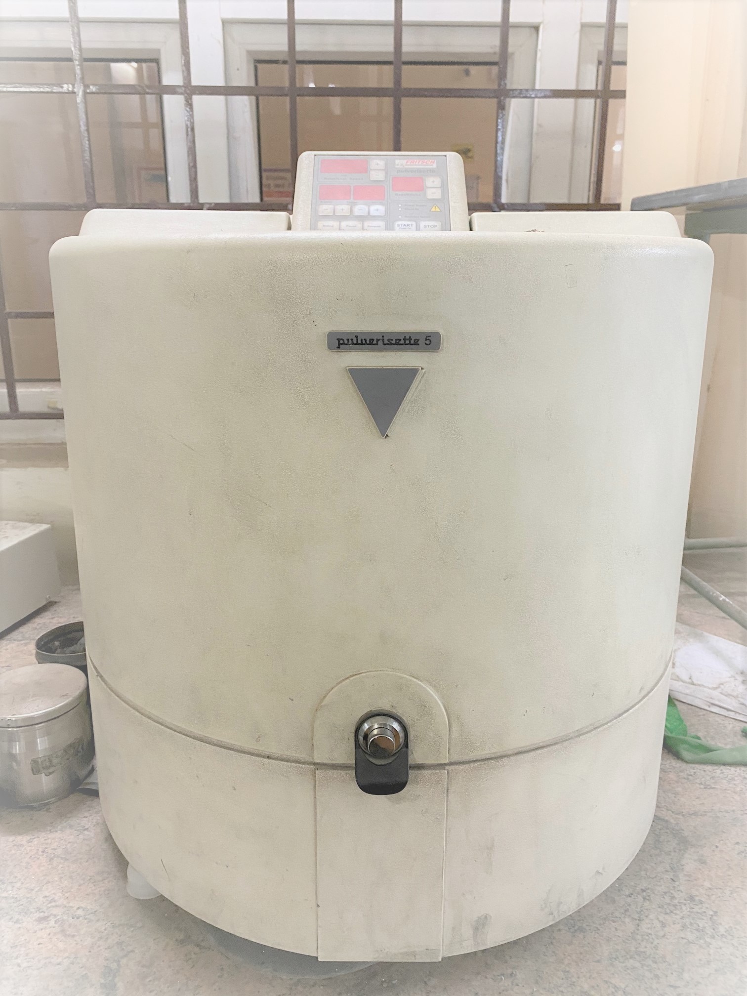
Fritsch Pulvert-5 High Energy Planetary Ball Mill

Maximum Speed – 400 RPM
Vials – WC, Stainless steel, Zirconia.
Balls (Ø10 mm) – WC, Stainless steel, Zirconia

Controlled Atmosphere Magnesium Melting Furnace

Maximum Temperature – 900°C
Atmosphere – Argon, SF6 and CO2
Casting – Bottom pouring

Stir Casting Facility

Maximum Temperature – 1100°C
Maximum Stirrer speed – 1500 RPM
Composites – Al/SiC, Al/Graphite, Al/MgAl2O4, Al/MgO, Al/TiB2 and Al/B4C

Pit type Melting furnace

Maximum Temperature – 1100°C
Heating Element – Kanthal
Atmosphere – Air

Melting and Heat treatment furnace

Maximum Temperature – 1400°C
Heating Element – Silicon Carbide
Atmosphere – Air

Spray Pyrolysis Set up

Application: Thin oxide films can be coated on substrates by spray pyrolysis method
Specimen temperature: 600° C
Work area: 300 x 300 mm
Spraying rate : 1 liter/hr (max)

Tubular Furnace

Application : Various materials (both nano and bulk) can be prepared under
various gas atmospheres
Maximum working Temperature: 1450°C
Sample area: 150 x 70 mm

Faculty In-charge : Dr. R. Selva Kumar

Indigenous electrospinning facility with flat plate and rotary drum collectors which can produce nanofibres from various organic and inorganic materials.

  • Flow control: 0.1 – 99.9 ml/h
  • Voltage source: 0 – 50 kV
  • Needle diameter : 50 – 1000 µm
  • Needle to collector distance: variable (1 – 30 cm)
  • Collector type: Plate, Slot, Drum, Conveyor and Disc type
  • Drum/disc rpm: variable (100 – 2000 rpm)
electrospinning

Faculty In-charge : Dr.R. Pavul Raj

Mbraun Glovebox

Model: Mbraun Unilab (1200/780)
Application: The Glovebox provides a dry and inert atmosphere to carry out air and moisture sensitive reactions.

Newport Low Cost Solar Simulator

Model: 96000, 150W.
Application: Offers the light similar to solar radiation. Used for testing the solar cells efficiency.

Clinical centrifuge

Application: To settle down the Nanoparticles
RPM: 4900
Capacity: 6 x 15 ml

Electrochemical Work Station, Make: BioLogic Science Instrument

Application: Electrochemical work station is a sophiscated instrument consisting of five channels. It consists of a potentiostat with a booster connected for low and high current applications. Using this instrument, we can perform testing on fuel cell and water electrolyser electrodes using techniques like cyclic voltammetry, Electrochemical Impedance Spectroscopy and corrosion studies. Charge – discharge measurements of batteries can also be performed using this work station.

Microwave oven

Application : To prepare Nanomaterials
Operating temperature: 220 deg C (max)
Frequency: 2.45 GHz

Faculty In-charge : Dr. P. Biji

Mbraun Glovebox

The Nanosensor Laboratory is equipped with the state-of-art facilities for fabrication, testing and calibration of gas sensors and electrochemical sensors. The sensor group focusses on implementing innovative ideas based on Nanotechnology to realize nanosensor devices for real time applications.

Faculty In-charge : Prof. K K Venkataraman

A cyber-physical system is a mechanism that is controlled or monitored by computer-based algorithms, integrated with the Internet and its users. These systems will be able to deliver new levels of performance and efficiency in physical processes. Cyber-physical systems engage with the real world in real time and complimented with Internet of Things (IoT) has applications in every engineering domain. Interesting applications of Cyber-Physical systems include Healthcare, Robotics, Automotive, Industry 4.0 applications and many more,

Projects
IoT interface for Nano sensors

The electronics’ interface that handles the sensor signals and convert them for display are enabled
for viewing/analysisng through the IoT platform using Bluetooth. The inputs of the system are
standardized to handle resistance variation or voltage variation from sensor.

High end ICU ventilator with IoT

High end ICU ventilator has been developed with 15” touch screen, ARM micro controller board,
Precision pneumatics and a special weaning algorithm. This unit is now interfaced to outside
world through Wi-fi for emergency communication to nurses, analysis on the network and the health of the unit.

Cyber system integrated Ammonia leak detection installation

The project was carried out in a local industry, to reduce the risk factors in isolated areas having large gas installations by detecting the leakages and displaying the status on a continuous basis. Leakage of gas can occur at multiple points in the same installation. Hence multiple sensors are interfaced to detect the leakage and transmit the signals to the base stations located far away. Using microcontrollers, multiple sensor values are received and processed. The processed data is encoded and transmitted to the base using wireless protocol where another microcontroller system decodes it and gives the respective sensor status. The system also provides an audio and visual warning when leakages are detected and since the time taken to detect is low due to high speed processing, the leakage situations are brought under control with minimum or no damage. This project is an economical and efficient method to reduce gas leakage risk in large instlllations using latest IoT technologies and monitoring anywhere in the web.

Industry 4.0 applications

wpChatIcon